

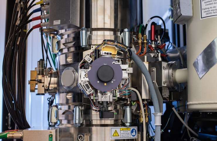
A significant part of the work was carried out at Linköping University on Arwen, one of the world's most distinguished transmission electron microscopes. A new method for assembling semiconductor layers as thin as a few nanometers has resulted not only in a scientific discovery, but also in a new type of transistor for high-powered electronic devices. The result, published in Applied Physics Letters, sparked great interest.
This success is the result of a close collaboration between scientists at Linköping University and SweGaN, a company from materials science research at LiU. The company produces special electronic components from gallium nitride.
Electric Vehicles
Gallium nitride, GaN, is a semiconductor used for efficient light-emitting diodes. However, it can also be useful in other applications such as transistors, as it can withstand higher temperatures and current forces than other semiconductors. These are important features not only for those used in electric vehicles, but also for future electronic components.
Gallium nitride vapor is allowed to condense on a plate of silicon carbide, forming a thin coating. The method by which one crystalline material is grown in the substrate of another is known as "epitaxy". The method is often used in the semiconductor industry because it provides great freedom in determining both the crystal structure and the chemical composition of the resulting nanometer film.
The combination of gallium nitride, GaN and silicon carbide SiC (both of which can withstand strong electric fields) makes the circuits suitable for applications requiring high power.
However, the harmony on the surface between the two crystalline materials, gallium nitride and silicon carbide, is weak. The atoms do not match each other, which leads to the failure of the transistor. This was addressed through research that led to a commercial solution in which a thinner layer of aluminum nitride was placed between two layers.
Engineers at SweGaN realized that their transistors could handle significantly higher field forces than they expected, and they initially couldn't figure out why. The answer can be found at the atomic level at several critical interfaces inside the components.
Transmorphic Epitaxial Growth
At LiU and SweGaN, LiU's researchers led by Lars Hultman and Jun Lu presented an explanation of the phenomenon in Applied Physics Letters and described the method of producing transistors that are more capable of withstanding high voltages.
Scientists have discovered a previously unknown mechanism of epitaxial growth, which they call "transmorphic epitaxial growth." It causes the tension between the different layers to be gradually absorbed through several layers of atoms. This means that at the atomic level they can grow two layers, gallium nitride and aluminum nitride, on silicon carbide to control how the sheets relate to each other within the material. In the laboratory, they showed that the material withstands high voltages up to 1800 V. If such a voltage is placed on a classical silicon-based component, sparks will begin to fly and the transistor will be destroyed.
Lars Hultman: "We congratulate SweGaN on launching the invention. It demonstrates effective collaboration and the use of research results in society. Because of our close contact with our previous colleagues who are currently working for the company, our research is having a rapid impact outside the academic world as well."